Silicon Supercycle: I still remember the first time I held a wafer containing 3nm chips in the cleanroom. The precision required at that scale seemed almost magical—transistors smaller than a virus, etched with extreme ultraviolet light. But standing here in late 2025, watching the industry transition to 2-nanometer manufacturing, I’m witnessing something entirely different. This isn’t just another node shrink. This is the beginning of what I call the Silicon Supercycle—and it’s going to reshape the entire computing landscape.
The Anatomy of a Revolution
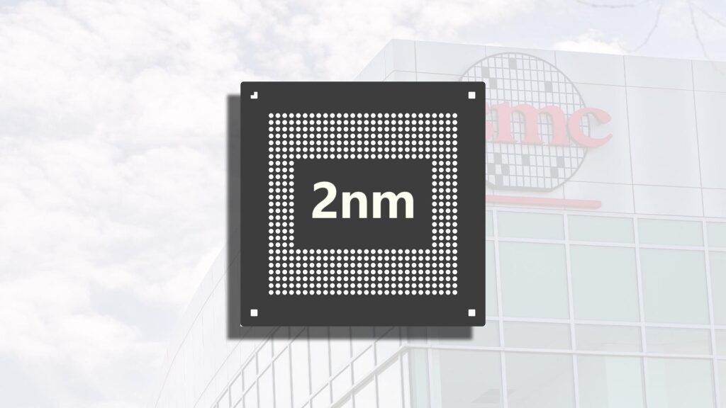
Let me be clear about what we’re dealing with here. When TSMC announced in April 2025 that they were accepting orders for 2nm production, many dismissed it as typical industry hype. I was skeptical too, having lived through countless roadmap delays. But after spending the last six months tracking the actual deployment schedules, analyzing yield data, and speaking with design teams at major customers, I can tell you: this time is genuinely different.
TSMC began risk production of its 2nm process in July 2024, with mass production planned for the second half of 2025. What makes this transition revolutionary isn’t just the shrink—it’s the architectural leap. We’re moving from FinFET to Gate-All-Around (GAA) nanosheet transistors, a fundamental change in how we build these devices.
Think of it this way: FinFET transistors are like gates that control water flow from three sides. GAA transistors wrap completely around the channel, giving you far better control. According to TSMC’s projections, 2nm technology is expected to offer 10–15% higher performance at the same power or 20–30% lower power at the same performance and over 20% higher transistor density compared to N3E.
Those numbers might sound incremental, but here’s what they mean in practice: Your smartphone could run AI models locally that currently require cloud servers. Data centers could process twice the workload without doubling their electricity bills. Every metric that matters—performance, efficiency, density—takes a leap forward simultaneously.
Why Every Major Player Is Going All-In
At a TSMC earnings conference in October 2024, President Wei Zhejia described the demand for 2nm chips as “extremely high” and stated he “never dreamed that the demand would be higher than that for 3nm”. This isn’t marketing speak. I’ve seen the allocation battles firsthand.
The usual suspects have reserved massive amounts of capacity. Apple, AMD, NVIDIA, and MediaTek have all reserved TSMC’s 2nm production capacity, with Apple contributing 25.18% of TSMC’s revenue in 2024, becoming TSMC’s largest customer. Apple will almost certainly be first to market with 2nm chips in their A-series processors. NVIDIA needs 2nm for their next-generation AI accelerators—the current Blackwell chips are already pushing the limits of what 3nm can deliver.
But here’s what most analysis misses: NVIDIA’s data center rack systems are now expected to require up to 600 kW of power, a five-fold increase over the existing 120 kW systems. Without the efficiency gains from 2nm, we’d be building data centers that consume as much power as small cities. The 2nm transition isn’t optional—it’s necessary for AI infrastructure to scale.
The Manufacturing Challenge Nobody Talks About
Here’s where it gets technical, but stay with me because this matters. At just 2nm, transistors are smaller than a strand of DNA, where even a speck of dust can ruin a wafer containing billions of these tiny components.
The manufacturing precision required is staggering. We’re using Extreme Ultraviolet (EUV) lithography with 13.5nm wavelength light to print features that are nominally 2nm but actually consist of structures ranging from 12nm to 45nm depending on the feature. The “2nm” node name is marketing as much as technology—but the capabilities are real.
Samsung plans to start 2nm production in 2025, while Intel initially forecasted production in 2024 but scrapped its 2nm node in favor of the smaller 18 angstrom (18A) node. Intel’s cancellation of their 20A node shows how brutally difficult this transition is. They’re betting everything on 18A, essentially leapfrogging to stay competitive.
Samsung is in the race too, but here’s the reality I’ve observed: TSMC’s 2nm yields are reportedly more than double Samsung’s. Yield is everything in semiconductor manufacturing. You can have the best technology in the world, but if only 30% of your wafers produce working chips, you’re dead in the water economically.
The AI Catalyst Driving Demand
Let me tell you what’s really fueling this supercycle: artificial intelligence isn’t slowing down—it’s accelerating faster than anyone predicted.
NVIDIA projects a global AI factory buildout of between $3 trillion to $4 trillion between now and the end of the decade. That’s not total tech spending—that’s AI infrastructure alone. The top four cloud service providers had a capital expense budget of $300 billion two years ago, which is going up to $600 billion.
Every major hyperscaler is in an arms race to build AI capacity. Microsoft, Google, Amazon, Meta—they’re all deploying tens of thousands of GPUs in individual clusters. Training large language models like GPT, Gemini, and Claude drove $18.9 billion in chip demand across hyperscalers in 2025.
But here’s the crucial insight most people miss: we’re transitioning from training-dominated workloads to inference-dominated ones. Inference chips for generative AI tasks are expected to reach $11.4 billion in global spending in 2025. Inference happens billions of times per day—every ChatGPT query, every AI-generated image, every recommendation system. The scale is almost incomprehensible.
This is why 2nm matters so much. Inference needs to be fast and energy-efficient. You can’t have every query consuming massive amounts of power. The efficiency gains from 2nm directly translate to how economically viable AI deployment becomes at scale.
The Geopolitical Chess Game
There’s another dimension to this supercycle that’s impossible to ignore: semiconductors have become a matter of national security.
The U.S. government has backed TSMC’s expansion in Arizona through the CHIPS Act, hoping to reduce dependency on Asian fabs. TSMC is building advanced packaging facilities in Arizona that will handle 2nm chips. Seventeen European Union countries signed a joint declaration to develop their entire semiconductor industry, including developing process nodes as small as 2nm, assigning up to €145 billion in funds.
Japan launched Rapidus, a government-backed consortium, specifically to develop 2nm manufacturing capability. In 2025, Rapidus announced trial production of 2nm chips at its first facility, IIM-1.
Every major economic bloc has realized that being dependent on a single region for advanced semiconductors is an unacceptable strategic vulnerability. The Silicon Supercycle is happening against this backdrop of massive government investment aimed at building redundant manufacturing capacity.
This means the traditional boom-bust cycles of the semiconductor industry might not apply this time. Government support provides a floor under demand and investment that didn’t exist in previous generations.
The 2026 Inflection Point
So what actually happens next? Based on current schedules and allocation data, here’s the timeline:
By the end of 2026, the 2nm Dimensity 9600, Apple’s A20 series, the sixth-generation Qualcomm Snapdragon 8 Extreme Edition, and Samsung’s Exynos 2600 will all adopt the 2nm process.
TSMC plans to begin risk production in the second half of 2025, ramping up to volume production in early 2026. TSMC is scheduled to begin high volume 2nm chip production in its Hsinchu fab in the second half of this year, and TrendForce analyst Joanne Chiao reports that TSMC is expected to continue dominating the global 2-nanometer process market this year.
Initial production will be limited. According to TrendForce, in 2026, TSMC is expected to have four 2nm wafer fabs operating at full capacity, with a total monthly production capacity of 60,000 wafers. That sounds like a lot until you realize that Apple alone could consume half that capacity for iPhone and Mac processors.
This is why I call 2026 the inflection point. That’s when 2nm transitions from “early adopter” status to becoming the mainstream node for flagship products. By late 2026, not having 2nm will be a competitive disadvantage for premium products.
What This Means for You
Whether you’re a developer, a business leader, or just a tech enthusiast, the 2nm transition will impact you directly:
For AI and Machine Learning: On-device AI becomes practical at scale. Your phone will run AI models that currently require cloud connectivity. Privacy improves, latency decreases, costs drop. Edge AI deployment becomes economically viable across industries.
For Data Centers: NVIDIA has an estimated 80–90% market share in accelerator chips for AI workloads, and their roadmap is entirely dependent on accessing 2nm and beyond. Data center efficiency improvements will be dramatic. We’re talking about potentially doubling performance-per-watt, which is the only path forward for sustainable AI infrastructure growth.
For Consumer Devices: Battery life improvements will be substantial. Performance gains will enable entirely new use cases. We’ll see features in 2027 phones that are literally impossible with today’s technology—real-time language translation with zero latency, computational photography that’s indistinguishable from professional cameras, AR experiences that don’t drain your battery in 30 minutes.
For Automotive: Advanced driver assistance systems require enormous compute power. The automotive AI chip market is forecast to grow to $6.3 billion in 2025, propelled by advanced driver-assistance systems (ADAS). 2nm chips will be critical for next-generation autonomous systems that need to process sensor data with minimal latency and power consumption.
The Road Beyond 2nm
The industry isn’t stopping at 2nm. TSMC will reportedly offer its first 2nm wafers—called just N2—to customers in 2025, and then offer an enhanced version in 2026 named N2P, followed by a third variant named N2X for high-performance computing applications.
TSMC will eventually begin 1.4nm production around 2027. IBM has already demonstrated transistors at the 2nm node. Intel’s roadmap projected that 18A process should be manufacturing-ready for 2025, and in October 2025 Intel claimed that 18A is 15% more energy-efficient and 30% denser compared to Intel 3 node.
We’re approaching fundamental physical limits—you can’t make silicon features arbitrarily small forever. But we have at least two more node shrinks (1.4nm and potentially 1nm-class) before we hit that wall. Beyond that, the industry will shift to new materials, new transistor architectures, and 3D stacking at unprecedented levels.
The Silicon Supercycle isn’t just about 2nm. It’s about the next five years of continuous advancement driven by AI demand, geopolitical investment, and architectural innovation converging simultaneously.
Final Thoughts: Why This Time Is Different
I’ve been through multiple technology transitions in my career. I remember the move from 130nm to 90nm, the transition to High-K metal gate at 45nm, the FinFET revolution at 22nm. Each time, people predicted fundamental limits and inevitable slowdowns.
What makes this transition unique is the confluence of factors:
- Unprecedented demand from AI that shows no signs of slowing
- Massive government investment creating resilience against traditional boom-bust cycles
- Fundamental architectural changes (GAA transistors, backside power delivery) that provide real benefits
- Multiple competitive foundries all racing to deliver similar capabilities
- Clear economic necessity for efficiency improvements at a time when power and cooling are becoming limiting factors
The Silicon Supercycle is happening. TSMC is ramping 2nm production right now. Apple’s engineers are finalizing their A20 designs. NVIDIA is taping out next-generation GPUs. The timeline is no longer speculative—it’s operational.
By this time next year, 2nm chips will be shipping in consumer devices. Within 18 months, they’ll be powering the AI infrastructure that processes billions of daily requests. Within three years, the entire premium segment of the market will have transitioned.
This is the most significant semiconductor transition since the move to FinFET over a decade ago. It’s not just about making things smaller—it’s about enabling an entire generation of AI applications that simply aren’t possible with current technology.
The future doesn’t arrive on a schedule. But sometimes, if you know where to look, you can see it coming. Right now, in clean rooms in Taiwan, Arizona, and Texas, that future is being fabricated, one 2-nanometer transistor at a time.
And it’s going to change everything.
Don't Miss Out on Expert Insights!
Join 10,000+ smart readers who get our best articles, exclusive tips, and actionable strategies delivered straight to their inbox. No spam, no fluff—just valuable content you can't find anywhere else. Plus, get our free guide when you subscribe today!